Top-Level Architecture
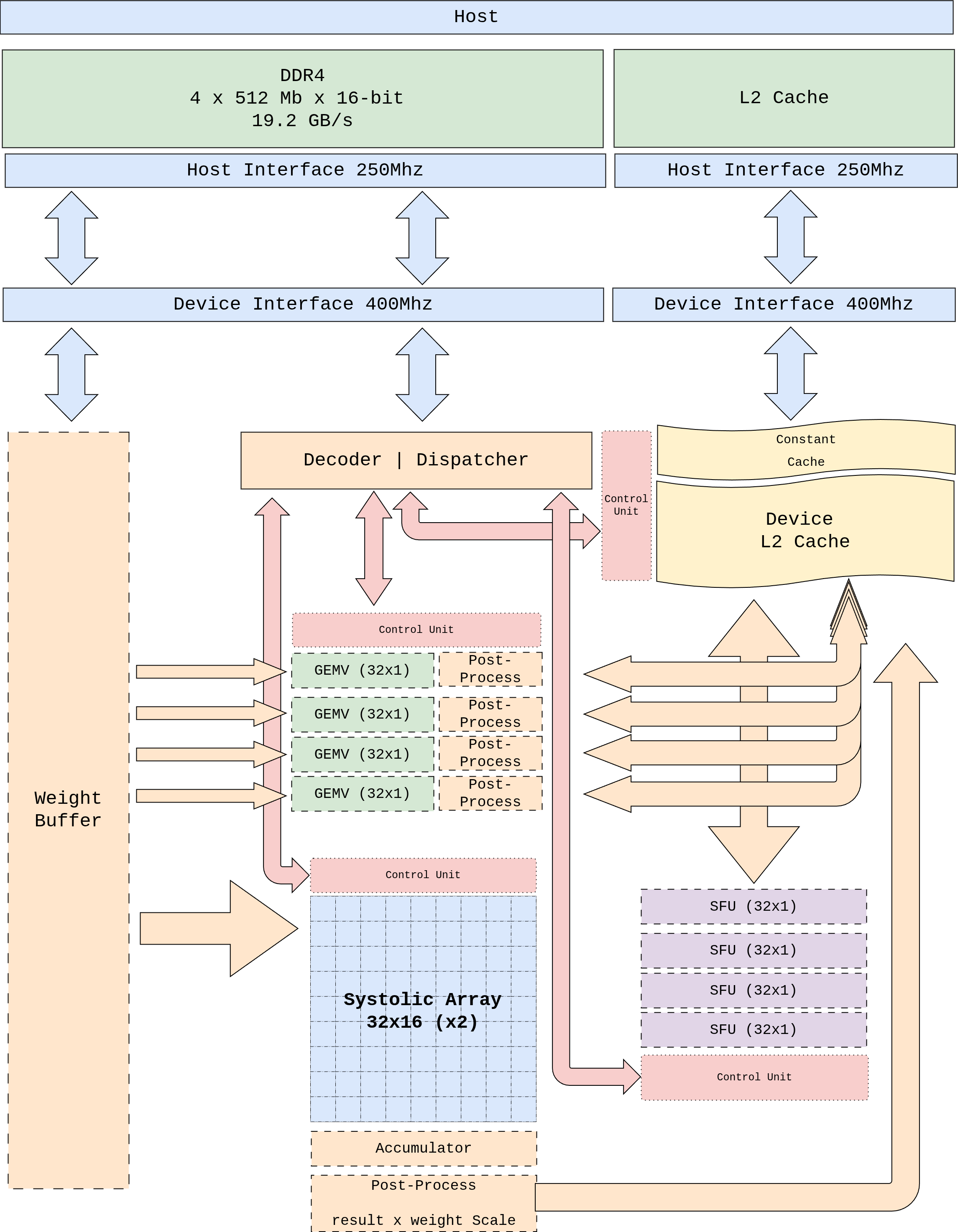
Figure 1 Figure 1. pccx v002 top-level block diagram. Shows the data path between host DDR4 and the device-side L2 cache, the clock domain crossings, and the placement of each heterogeneous compute core.

Figure 2 Figure 2. System context. The AXI-Lite command path (CMD_IN)
carries 64-bit instructions from the host driver into the Control
Unit + Dispatcher; the dual-direction AXI-Lite STAT_OUT reports
async completion. Four 128-bit AXI-HP ports plus one ACP port move
the bulk data (weights, activations, KV cache) between external
DDR4 and the AXI Interconnect. Inside the PL, the Dispatcher fans
μops out over a single trunk to the GEMM, GEMV, SFU, and DMA
back-ends, which read and write through the L1 Weight Buffer and
the L2 cache.
1. Design Principles
The top level is organized around four principles.
Clock domain separation — The AXI infrastructure (250 MHz) is decoupled from the core logic (400 MHz) so that AXI protocol timing never constrains the core frequency.
Decoupled dataflow — Instruction decode (front-end) and execution (back-end) are separated by an asynchronous FIFO, eliminating pipeline stalls due to dispatch latency.
Separated weight and activation paths — Weights stream directly from host DDR4 into the weight buffer, while activations flow from the central L2 cache. The two streams never collide on the interconnect.
Centralized L2 cache — GEMM, GEMV, and SFU are placed physically close to L2, eliminating the cost of reshuffling activations between layers.
2. Major Blocks
Block |
Domain |
Role |
|---|---|---|
Host Interface |
250 MHz |
AXI-Lite (control registers), AXI HP ports (data streaming), AXI ACP (host-cache DMA). Bridged to the 400 MHz domain through a CDC FIFO. |
Device Interface |
400 MHz |
Core-side AXI slave. Bridges onto the Weight Bus and the L2 cache R/W ports. |
Decoder / Dispatcher |
400 MHz |
Decodes 64-bit instructions and emits per-opcode control μops. See Instruction Encoding. |
Control Unit |
400 MHz |
Global scheduler. Handles dependency resolution, dispatch ordering, and completion notification. |
Weight Buffer |
400 MHz |
Broadcasts INT4 weights streamed in from the HP ports to the GEMM / GEMV cores. |
L2 Cache |
400 MHz |
Central shared cache. Stores activations, intermediate results, and the KV cache. |
Constant Cache |
400 MHz |
Stores small constants — shape / size pointers, scale factors — written by MEMSET. |
Systolic Array (32 × 32, cascade break @ row 16) |
400 MHz |
GEMM-only 2D systolic array. Single instance; two 32 × 16 sub-chains share the grid. See GEMM Core (Systolic Array). |
GEMV Core (×4) |
400 MHz |
Four parallel cores, each a 32-MAC LUT pipeline + 5-stage reduction tree. See GEMV Core. |
SFU (×1) |
400 MHz |
A single scalar BF16 pipeline (1 element / clk) for Softmax, GELU, RMSNorm, RoPE, and friends. See SFU Core (Complex Vector Operations). |
3. Clock Domain Strategy
3.1 Why Split the Domains
The KV260 AXI interconnect closes timing comfortably at 250 MHz, but the core logic — when all DSP48E2 pipeline stages are enabled — can reach 400 MHz. Separating the two lets each subsystem run at its natural rate:
AXI domain (250 MHz): Host, DMA, AXI-Lite control register access.
Core domain (400 MHz): Dispatcher, Control Unit, every compute core, L2 cache.
3.2 CDC (Clock Domain Crossing)
The domain boundary is crossed through an asynchronous FIFO. Each
AXI HP port delivers bursts at burst_length × AXI_clock bandwidth,
sized so that the 400 MHz core side is never starved. See the bandwidth
matching analysis in Memory Hierarchy.
4. Data Path Summary
        flowchart LR
  DDR[(Host DDR4)] -->|HP2/HP3| WB[Weight Buffer]
  DDR -->|ACP DMA| L2[(L2 Cache<br/>Central URAM)]
  WB --> SA[Systolic Array<br/>32×32]
  WB --> GV[GEMV Core<br/>×4]
  L2 --> SA
  L2 --> GV
  L2 <--> SFU[SFU<br/>×1]
  GV <-. direct FIFO .-> SFU
  SA --> L2
  GV --> L2
  SFU --> L2
  DISP[Decoder / Dispatcher] -->|μop| SA
  DISP -->|μop| GV
  DISP -->|μop| SFU
  DISP -->|MEMSET| CC[Constant Cache]
Instruction |
Primary Data Path |
Notes |
|---|---|---|
GEMM |
Weight Buffer → Systolic Array ← L2 |
Prefill stage. Weights and activations meet inside the array. |
GEMV |
Weight Buffer → GEMV Core ← L2 |
Decoding stage. Four GEMV cores partition across batch / head. |
CVO (SFU) |
L2 ↔ SFU, with direct GEMV ↔ SFU FIFO |
Weight path unused. Softmax / GELU / RoPE. |
MEMCPY |
Host DDR4 ↔ L2 |
ACP port. Synchronous or asynchronous. |
MEMSET |
Dispatcher → Constant Cache |
Initializes small constants — shape / size pointers and the like. |
For per-instruction dataflow detail, see Per-Instruction Dataflow.