GEMM Core (Systolic Array)¶
The GEMM core handles the large matrix-matrix multiplications that dominate the prefill stage of a Transformer. pccx v002 uses one 32 × 32 2D systolic array whose accumulation cascade is broken at row 16, giving two 32 × 16 sub-chains that share the same physical grid and deliver a theoretical peak of 819 GMAC/s at 400 MHz.
Note
GEMM is used mainly in prefill (long-prompt initial processing) and in
Attention’s Q·Kᵀ and score·V. For the decoding-dominant GEMV
operation, see GEMV Core.
1. Operands¶
GEMM computes the product of a Weight (N × N) matrix and an Activation (N × N) matrix.
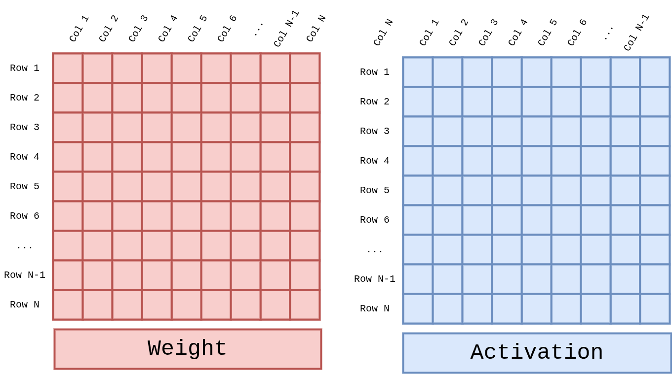
Figure 3 Figure GEMM-Operands. GEMM takes two 2D tensors (weight and activation) and produces a partial-sum result. Both operands are defined as Row × Col; tile shapes are chosen by the software layer.¶
2. Array Configuration¶
Parameter |
Value |
|---|---|
Physical grid |
32 (M) × 32 (K) → 1,024 PEs |
Cascade break |
at row 16 → two 32 × 16 sub-chains ( |
DSP per PE |
1 (DSP48E2) |
MAC / clk per PE |
2 (dual-channel bit packing, see DSP48E2 W4A8 Bit Packing and Sign Recovery) |
Total MAC / clk |
1,024 PE × 2 MAC = 2,048 |
Peak throughput |
2,048 × 400 MHz = 819 GMAC/s |
3. Array Structure and Dataflow¶
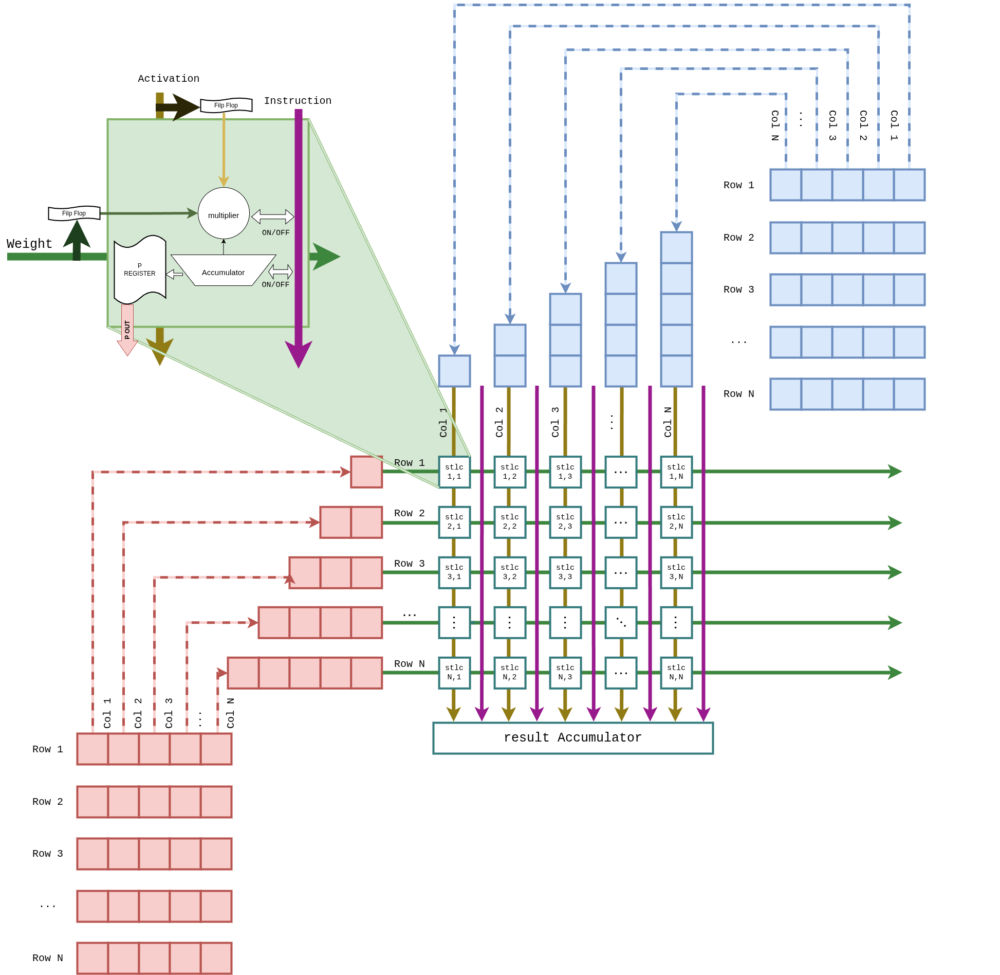
Figure 4 Figure GEMM-Array. The systolic array is a Weight Stationary structure: weights enter from the left, activations from the top, and partial sums collect in the Result Accumulator at the bottom. The zoomed-in green box shows the internals of a single PE.¶
3.1 Weight Stationary Reuse¶
During GEMM, the same weights are reused across many activation tiles. Rather than re-reading weights from the HP ports for every tile, we preload them into the flip-flops inside each PE.
The Weight Buffer pulls a tile’s worth of INT4 weights from the HP ports.
The Weight Dispatcher staggers the loads and places them on each PE’s Port A.
Port A is packed as {W₁ | 19-bit guard | W₂} for dual-channel packing (DSP48E2 W4A8 Bit Packing and Sign Recovery §2).
The same weights are reused for the full activation tile sweep.
3.2 Activation Streaming¶
The relevant INT8 activation tile is streamed from the L2 cache into the top of the systolic array.
A per-column fmap staggered delay keeps pipeline timing aligned.
Activations propagate top-to-bottom through the array; the output row axis maps onto the array’s column direction.
        flowchart LR
  subgraph Host[Host DDR4]
    W[Weights INT4]
  end
  WB[Weight Buffer<br/>URAM FIFO] -->|staggered| PE[(PE Grid<br/>32×32 · cascade break @ row 16)]
  L2[L2 Cache<br/>URAM] -->|activations INT8| PE
  PE -->|partial sums| RA[Result Accumulator]
  RA -->|scale / requant| L2
  W --> WB
3.3 Accumulation¶
Partial sums accumulate into the DSP48E2’s 48-bit P register across K depth.
Dual-channel bit packing caps safe accumulation at
N_max = 2²² / 2¹⁰ = 4,096cycles.For K > 4,096, software tiles the layer (K-split).
3.4 Result Extraction & Sign Recovery¶
Once accumulation finishes, a single post-processing cycle separates the upper and lower channels and restores the borrow caused by a negative lower accumulator. The math and the Verilog implementation live in DSP48E2 W4A8 Bit Packing and Sign Recovery.
4. PE Microarchitecture¶
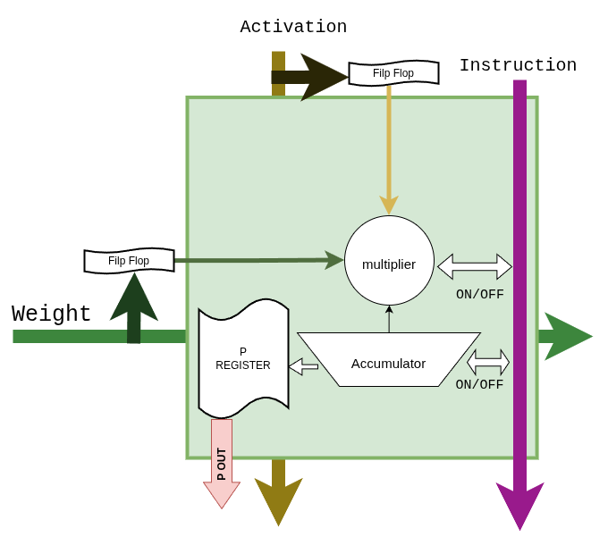
Figure 5 Figure GEMM-PE. A single PE consists of the weight / activation
input flip-flops, the DSP48E2 multiplier, the P register, the
accumulator, and on/off control signals. The Instruction port
carries μops extracted from the instruction (enable / flush /
accumulate-done), and P_OUT is active only when accumulation
completes, routing into the Result Accumulator.¶
Every DSP48E2 pipeline register is enabled to hit 400 MHz timing closure.
Stage |
Logic |
Description |
|---|---|---|
S0 |
Weight Register |
Latches both 4-bit weights in the 27-bit packed form. Stable during reuse. |
S1 |
Activation Register |
Receives an INT8 activation from the upstream neighbor PE. |
S2 |
DSP48E2 M stage |
Port A × Port B (27 × 18-bit) multiply. |
S3 |
DSP48E2 P stage (ACC) |
48-bit P register accumulation. ON/OFF control handles flush / hold. |
S4 |
Propagate |
Forwards the activation to the next PE. |
5. Post-Processing¶
Beyond the Result Accumulator, data flows through the following stages.
Stage |
Function |
|---|---|
Result Accumulator |
Collects PE results at the array boundary and performs the upper/lower channel split with sign recovery. |
Post-Process |
|
L2 Writeback |
Writes to the L2 cache address named by the ISA |
Relevant ISA flags are detailed in the GEMM section of Per-Instruction Encoding.
6. Scalability¶
The array dimensions are exposed as SystemVerilog generate
parameters.
Parameter |
KV260 default |
Meaning |
|---|---|---|
|
32 |
PEs in the weight / M direction ( |
|
32 |
PEs in the activation / K direction. Independent of the safe-accumulation limit. |
|
16 |
Fixed inside |
|
1 |
One |
On KV260 the 32 × 32 grid consumes 1,024 DSP48E2 slices — about 82 % of the device’s 1,248-slice budget.